Figure 4:
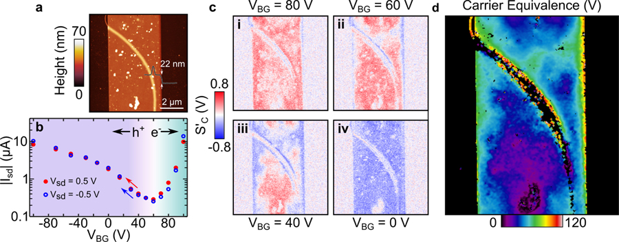
(a) AFM topography of a tellurene device with embedded Te filament. (b) Transport characteristics of the device with a global carrier equivalence point of VBG = 60 V. (c) Sequence of images that illustrates the high degree of spatial inhomogeneity in carrier type and density present in this device as further seen in (d), the extracted carrier equivalence map.

