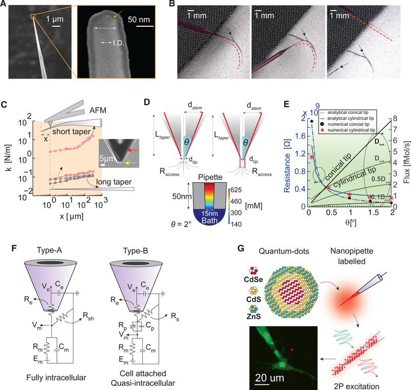
Figure 1. Flexible Nanopipette Design Characteristics.
(A) SEM of the nanopipette (left) and magnified view of the tip (right). The outer diameter-to-inner diameter (I.D.) ratio is 2:1. Note the outer 10 nm platinum coating layer required for SEM imaging.
(B) Images depicting the degree of nanopipette flexibility (left, middle, and right). The nanopipette (false colored; red dotted line) is immobilized on tape, and the taper is subsequently bent (left). The taper is bent farther (>60° ) (middle) and subsequently recovers to a taut axially stiff pipette (right) when removed from the tape without damage. The black arrows indicate imprints of the taper in the tape.
(C) AFM-based stiffness measurements of nanopipettes for varying taper lengths (black, blue, and red indicate a long nanopipette with small variations in taper length (~8 mm), and pink represents a short tapered conventional sharp microelectrode design). The inset depicts the AFM tip (red) scanning the tip of the nanopipette (yellow). The spring constant (stiffness) of the long tapered nanopipette close to the tip (~0.08 N/m) reveals a highly compliant structure.
(D) Geometry of the two types of nanopipettes commonly used: conical tip (upper left) and cylindrical tip with conical taper (upper right). The half cone angle (theta), length of the taper (Ltaper), diameter of the tip (dtip), and access resistance (Raccess) influence the net resistance, concentration gradient, and flux. Simulated heatmap of the concentration gradient at the tip of a purely conical nanopipette (bottom). Note the large gradient close to the tip.
(E) Numerical simulations of resistance versus theta (left y axis) and flux versus theta (right y axis) for the two geometries shown in (D) for a fixed diameter of 15 nm and 3 M KCl filling solution. Low flux values (<1 fM/s) can be achieved when the pipette tip is cylindrical (theta of ~0) near the end and the diffusion constant of ions at the tip (cytoplasmic fluid) is lower than bulk. Resistance versus theta was calculated analytically and corroborated numerically (see text for details).
(F) Equivalent circuit models showing the nanopipette cell membrane interface under full tip impalement (left, type A) and electroporation-induced or cell-attached entry (right, type B). Here, Re and Ce denote the distributed pipette resistance and capacitance, respectively. Rsh, Rs, and Rp represent the shunt, seal, and pore resistance, respectively. Rm represents the membrane resistance, Cm represents the membrane capacitance, Cp represents the pore capacitance, and Em represents the reversal potential of the leak channels. Depending on whether Rp or Cp dominates the junction contribution, and under a moderate to high Rs, the recorded signal Ve could reflect either a purely capacitive extracellular signal (Cp dominates, similar to cell-attached recording) or a tightly coupled and scaled intracellular signal (Rp dominates, similar to quasi-intracellular or in-cell recordings).
(G) CdSe/Cds/ZnS QDs label nanopipettes through adsorption, allowing clear visualization of the nanopipette relative to the patch pipette under two-photon visualization (bottom).

