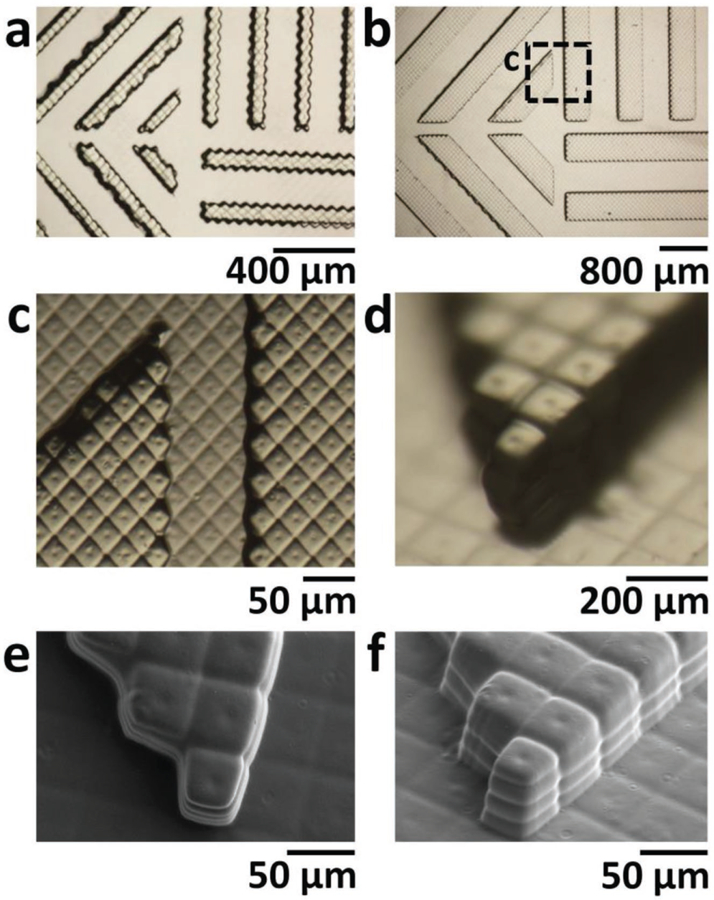
Figure 2.

X–Y resolution. a,b) Bright field micrographs of a) 2 pixel wide and b) 8 pixel wide, 200 µm tall lines that were 3D-printed horizontally, vertically, and diagonally in 50 µm thick Z-layers with 0.4% IRG and 0.4% ITX PEG-DA-258 resin. c) Magnification of the area boxed in (b). (d) Oblique-view bright-field micrograph of SL-printed 200 µm tall pixels at the corner of an 8 pixel wide diagonal line. Note how sub-pixel features in (c) and (d) are well defined. e) Top-view SEM image of pixels at the corner of an 8 pixel wide diagonal line. The image reveals the shape of sub-pixel features created by the topology of the DMD micromirrors: ≈10 µm diameter circular dimples at the center of each pixel and ≈5–10 µm wide lines between the pixels. f) Oblique-view SEM image of pixels at the end of an 8 pixel wide diagonal line where individual 50 µm thick layers can be seen as well as the sub-pixel features mentioned above.
