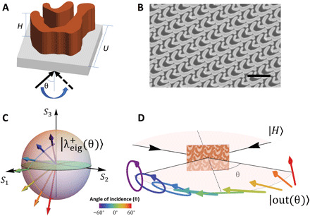
Fig. 2. Topology-optimized structure element.

(A) Schematic of the optimized structure. It consists of freeform amorphous silicon (a-Si) nanostructures patterned on top of a glass substrate. The a-Si thickness is H = 1500 nm. The center-to-center distance between neighboring elements is U = 600 nm. (B) SEM image of a fabricated sample. Scale bar, 1 μm. (C) The arrows represent the angle-dependent eigen-polarization states () of the device. Different colors correspond to different angles of incidence (θ). As one varies the angle, the device can be continuously tuned between linear and elliptical birefringence. (D) Angle-dependent polarization generation. For a fixed incident polarization (∣in⟩ = ∣H⟩), the output polarization state (∣out(θ)⟩ = J(θ)∣H⟩) changes continuously from right circular polarization through horizontal linear polarization to 45∘ linear polarization for varying angle of incidence.
