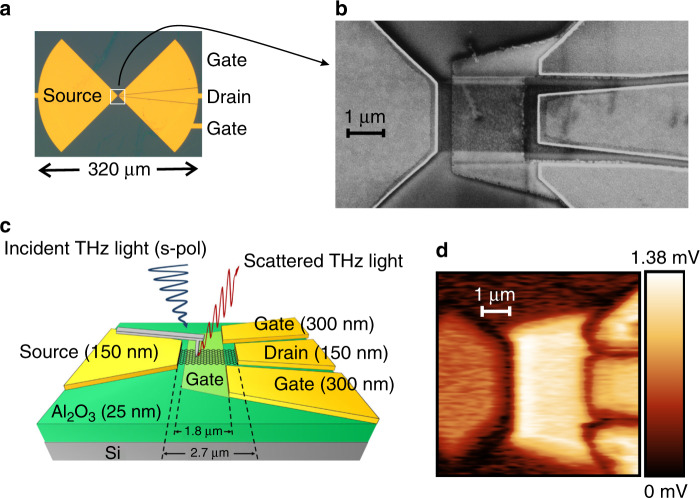
Fig. 1. Graphene TeraFET detector.
a Microscope image of the device showing the bow-tie antenna. b Scanning electron micrograph of the apex region of the antenna arms (region marked by the white box in a) showing the FET channel. The graphene layer on top of the buried gate can be clearly identified. c Schematic view of the channel region between the drain and source electrodes, specifying the thicknesses of the gold and Al2O3 layers. Also indicated is the cantilever of the s-SNOM. The cantilever arm is almost parallel to the symmetry axis of the antenna leaves. d Single-scan s-SNOM near-field image of the field distribution upon illumination with radiation at 2 THz (total time-averaged power: 45 mW, beam diameter: 1 mm), 2-Ω-demodulation, gate voltage Vg = 0 V, drain-source voltage Vds = 0 V and lock-in integration time of 50 ms. The color scale represents the output voltage of the lock-in amplifier, which is proportional to the local field amplitude

