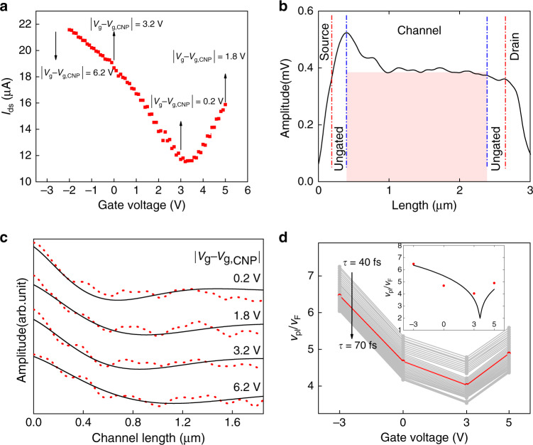
Fig. 2. Device 1.
a Drain-source current of the TeraFET when illuminated with 45mW of radiation at 2 THz (two traces). The arrows mark the voltage positions where s-SNOM line scans were performed. b 3Ω-near-field trace along the channel between the source and drain. Red dash-dotted vertical lines demark the edges of the source and drain electrodes; blue dash-dotted lines, the beginning and end of the gate electrode. The signal contribution attributed to the amplitude of the THz potential of the gate metallization is indicated by the colored rectangle. c Red-dotted lines: Near-field traces (zoomed-in on the plasma-wave component of the signal) for selected gate voltages indicated by the arrows in a. The curves are arranged in sequence of increasing value of from 0.2 V to 6.2 V. The curves are shifted vertically for clarity. Full black lines: calculated traces based on the fit function and the boundary conditions given in the Supplementary Materials (fit function: Eq. (7)). d Extracted νpl for values of τ between 40 fs and 70 fs. The red line represents νpl for τ = 55 fs. The inset compares the extracted values of νpl for τ = 55 fs (red dots) with the predictions of the theoretical model of refs. 18,43

