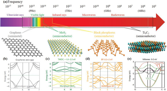
Figure 1.

Ultra‐broadband photoresponse of 2D materials from UV to microwave regime. a) Electromagnetic spectrum and the atomic structures of graphene, MoS2, and BP are shown in the bottom of the panel, left to right. The possible spectral ranges covered by different materials are indicated using colored polygons. Band structures of b) single‐layer graphene, c) MoS2, and d) BP. Reproduced with permission.[ 6 ] Copyright 2014, Nature Publishing Group. Reproduced with permission.[ 35 ] Copyright 2017, Springer Nature. e) Band structure of MXene monolayer with —OH and —F surface termination and no termination (Ti3C2). Reproduced with permission.[ 34 ] Copyright 2011, Wiley‐VCH.
