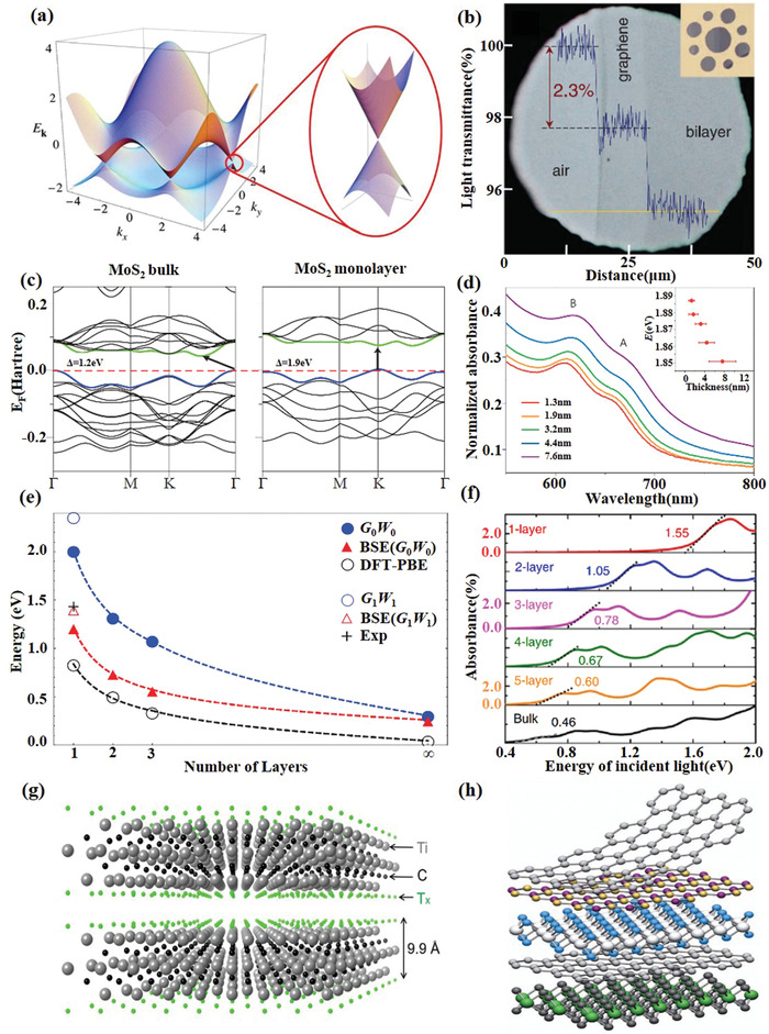
Figure 2.

Characterizations of types of 2D materials. a) Electronic band structure of graphene. Reproduced with permission.[ 16 ] Copyright 2009, American Physical Society. b) Light absorption of graphene monolayer. Reproduced with permission.[ 18 ] Copyright 2008, American Association for the Advancement of Science. c) The band structure of bulk and monolayer MoS2. d) Absorption spectra of MoS2 thin films with average thicknesses ranging from 1.3 to 7.6 nm. Reproduced with permission.[ 22 ] Copyright 2012, Nature Publishing Group. e) The evolution of bandgap calculated by different methods and optical absorption peak according to the stacking layer number of few‐layer phosphorene. Reproduced with permission.[ 25 ] Copyright 2014, American Physical Society. f) Optical absorption spectra of few‐layer BP for light incident. Reproduced with permission.[ 32 ] Copyright 2014, Nature Publishing Group. g) Crystal structure of typical MXene Ti3C2Tx. h) van der Waals heterostructure. Reproduced with permission.[ 4 ] Copyright 2013, Nature Publishing Group.
