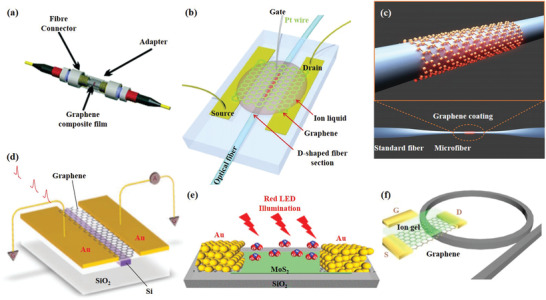
Figure 4.

Applications of typical 2D materials based optoelectronic structures. a) The SA material is deposited on the end of the fiber for ultrafast lasers. Reproduced with permission.[ 57 ] Copyright 2010, American Chemical Society. b) Graphene‐covered D‐shaped fiber for electro‐optic modulators. Reproduced with permission.[ 115 ] Copyright 2015, Nature Publishing Group. c) Schematic of a graphene‐clad microfiber all‐optical nonlinear devices. Reproduced with permission.[ 112 ] Copyright 2014, American Chemical Society. d) Integration of graphene and silicon waveguides for photodetectors. Reproduced with permission.[ 133 ] Copyright 2013, Nature Publishing Group. e) Au/MoS2/Au‐based BJT was deposited on SiO2 substrates for gas sensors. Reproduced with permission.[ 182 ] Copyright 2019, American Chemical Society. f) Schematic architecture of the graphene‐based microresonator. Reproduced with permission.[ 9 ] Copyright 2018, Springer Nature.
