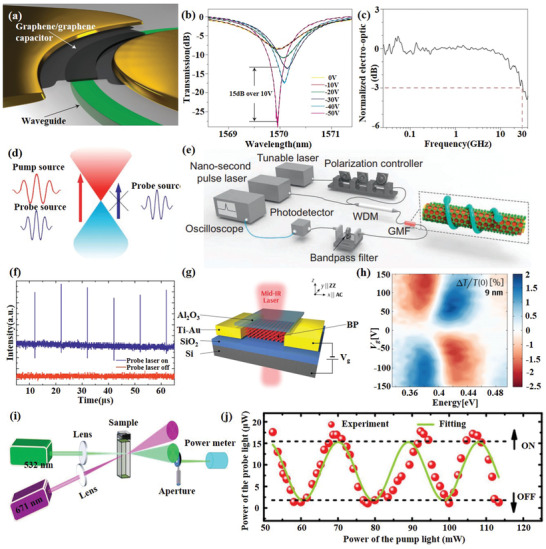
Figure 8.

2D material‐based modulators and switchers. a) Schematic of the modulator consisting of a graphene/graphene capacitor integrated along a ring resonator. b) Transmission spectra at various applied d.c. voltages. c) Electro‐optic frequency response with 30 GHz bandwidth. Reproduced with permission.[ 123 ] Copyright 2015, Nature Publishing Group. d) Schematic illustration of the all‐optical modulation mechanism. e) Schematic illustration of the all‐optical modulation measurement system. f) Time‐domain response of the GMF modulator. Reproduced with permission.[ 124 ] Copyright 2015, Nature Publishing Group. g) Schematic illustration of the BP modulator. h) The modulation level measured as functions of energy and gate bias for 9 nm thick BP. Reproduced with permission.[ 111 ] Copyright 2017, American Chemical Society. i) Ti3C2Tx MXene Ns‐based all‐optical switcher. j) The probe light modulated by the pump light to realize “ON” and “OFF” modes in all‐optical switcher. Reproduced with permission.[ 41 ] Copyright 2018, Wiley‐VCH.
