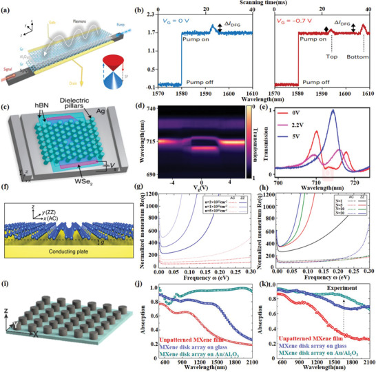
Figure 10.

2D material‐based plasmonic devices. a) Schematic of the dual‐layer graphene hybrid for difference frequency generation (DFG). b) Measured DFG‐based signal enhancement in the optical spectra. Reproduced with permission.[ 8 ] Copyright 2018, Springer Nature. c) A schematic of the plasmonic crystal cavity between two trenches etched in the silver that serve as in‐coupling and out‐coupling structures for surface plasmon polaritons (SPPs). d) Electrically tunable cavity transmission through a monolayer WSe2 as a function of gate voltage. e) Transmission spectra for three different gate voltages when the plasmonic crystal cavity is resonant with the exciton absorption in WSe2. Reproduced with permission.[ 158 ] Copyright 2019, American Chemical Society. f) Geometrical configuration supporting acoustic plasmons based on BP. g) Effect of electron density on plasmon dispersion. h) The effect of the number of layers on plasmon dispersion. Reproduced with permission.[ 159 ] Copyright 2018, American Chemical Society. i) Schematic of the MXene disk array. j) Simulated and k) Measured absorption spectra comparison of unpatterned MXene film, MXene 22 disk array on glass and MXene disk array on Au/alumina. Reproduced with permission.[ 164 ] Copyright 2018, American Chemical Society.
