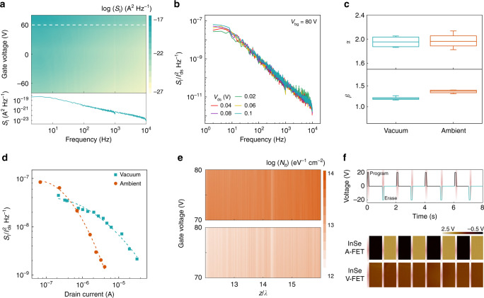
Fig. 3. Governing mechanisms of the carrier transport in InSe FET.
a Recorded SI as a function of frequency and gate voltages for InSe A-FET. Note that a SI curve at Vbg = 60 V based on the white dash line (upper) is profiled a representative of 1/f noise (under). b Drain current normalized SI depending on Ids for InSe A-FET at several Vds. c Box-plots of the fitted α (upper) and β (lower) values for InSe V- and A-FET. Note that the center line, the upper, and the lower bars correspond to the average, the maximum, and the minimum values, respectively. d Normalized SI by (discrete dots) versus Ids on a log-log scale for InSe FET under different conditions. The dashed lines are the well-fitted results based on the correlated mobility fluctuation. e The extracted values of effective interface trap density for InSe V- and A-FET as a function of z/λ and gate bias. f The dynamic variations of the surface potential (under read states) of InSe channel by in situ KPFM depending on the scanning time, for InSe A- and V-FET, respectively. The program and erase operations were defined by applying a +20 V and a –20 V gate voltage pulse (5 s) for 4 cycles.

