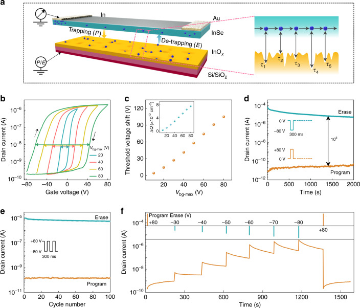
Fig. 4. Performance characterizations of the InSe A-FET based memory device.
a 3D schematic of InSe A-FET with the existence of InOx to achieve the charge trapping/ de-trapping under applied operation voltage. The inset on the right side delineates the uniform distribution of trapping states for the dynamic fluctuation process between the InSe channel and InOx layer. Note that τ means the time constant for different traps. b Transfer characteristics of InSe A-FET with the Vbg-max (the maximum value of the swept range of gate voltage). The drain voltage is set as 0.1 V and the colourful arrows mark the increasing threshold voltage shift. Note that the arrows indicate the directions of hysteresis loops. c Variation of the threshold voltage shift depending on Vbg-max. Inset shows the extracted amounts of trapped charges under various Vbg-max. d Retention performance of InSe A-FET based memory. The currents were separately read under Program and Erase states with Vds = 0.1 V and Vbg = 0 V. e Endurance characteristics of the memory device. Program and Erase operations were carried out under cyclic voltage pulses. The Read state was operated under Vds = 0.1 V. f Evolution of read current of the memory device under various operation states, which indicates its multiple data storage characteristics.

