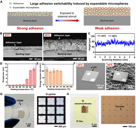
Fig. 1. The mechanism of shape-conformal stamp with large adhesion switchability and demonstrations for transfer printing of ultrathin Si nanomembranes.

(A) Schematic illustration of the novel concept design to construct a shape-conformal stamp with large adhesion switchability. (B) SEM images and (C) corresponding profile of TRT stamp before and after heating on a hotplate. (D) The measured surface roughness of the TRT stamp and (E) energy release rate of the TRT stamp with the glass slide after being uniformly heated on a hotplate at various temperatures. (F) SEM images of the ultrathin, inorganic μ-LED (285 μm by 285 μm by 4.6 μm) on the TRT stamp before and after heating on a hotplate, respectively. (G) Optical image of transfer-printed ultrathin Si pellets (400 μm by 400 μm by 200 nm) on the PDMS substrate under bending deformation. (H) Optical image of large-area Si nanomembrane (2 cm by 2 cm by 3 μm) transfer printed onto the PI substrate. Photo credit: C.W. and C.Lin., Zhejiang University.
