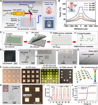
Fig. 2. Programmable transfer printing of Si nanomembranes and Si nanomembrane–based photodetectors.

(A) Schematic prototype of the laser-assisted programmable transfer printing system via automated translational stage. (B) Temperature increase at the interface of the TRT stamp and Si ink under various laser powers. (C) Schematic illustration of the programmable transfer printing process: (i) preparing Si pellets on an SOI wafer, (ii) picking up Si pellets using TRT stamp, (iii) programmable heating of Si pellets, and (iv) printing Si pellets on PDMS substrate. (D) Optical images of the programmable transfer printing process. (E) The selectively printed Si pellets on an Ecoflex-coated glass tube. (F) The magnified microscopic images corresponding to (D). Scale bars, 350 μm. (G) Maximum principal strain distribution of Si pellets under the bending radius of 1.5 mm. (H) Selectively printed Si nanomembrane–based photodetectors with a robot-like pattern on PDMS substrate. (I) Dynamic response of photodetector at various given light intensities and (J) measured I-V curve of the photodetector before and after transfer printing on PDMS receiver substrate. Photo credit: C.W. and S.N., Zhejiang University.
