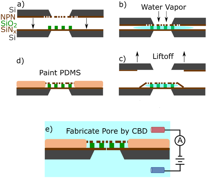
Figure 1:
A schematic illustrating of the assembly of the entropic trap. a) two chips containing an intact 20 nm thick SiNx sensing membrane decorated with an 800 nm SiO2 spacer containing a hexagonal grid of 4.5 μm microwells is brought into close proximity with a NPN membrane. b) water vapour floods the cavity and provides a weak adhesion force between the two membranes. c) the NPN support chip is lifted off, leaving behind the NPN layer capping the trapping cavities. d) Polydimethylsiloxane (PDMS) is painted around dual membrane stack, and over some of the interface to reduce device capacitance and permanently bond the two membranes. e) A nanopore is formed in one of the cavities at random using controlled breakdown.

