Figure 3.

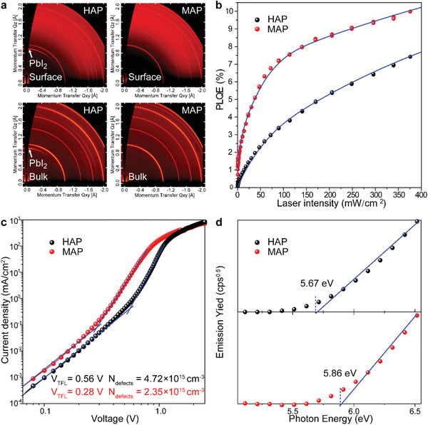
Contrast of structural anisotropy and electrical properties between optimized MAP‐30s and HAP‐30m perovskite films. a) 2D‐GIWAXS patterns of bulk‐phase and top‐surface, b) PLQE spectra, c) dark J−V curves, and d) IPS spectra.

Contrast of structural anisotropy and electrical properties between optimized MAP‐30s and HAP‐30m perovskite films. a) 2D‐GIWAXS patterns of bulk‐phase and top‐surface, b) PLQE spectra, c) dark J−V curves, and d) IPS spectra.