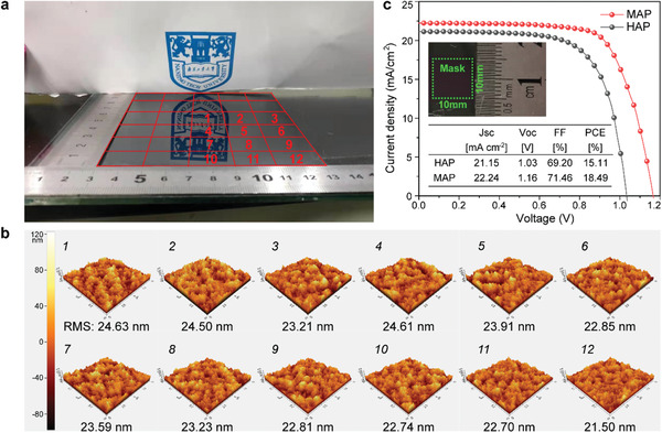
Figure 5.

Large‐scale fabrication of perovskite films and PSCs. a) Photograph of 10 cm × 10 cm perovskite film treated by MAP. Twelve different positions located from the center to the corner of this large‐size perovskite film were selected to be further tested. b) AFM topography images and root mean square (RMS) surface roughness from 12 different spots. c) Typical J–V curves and extracted PV parameters for HAP and MAP‐PSCs with the active areas of 1 cm2 as shown by the inset picture.
