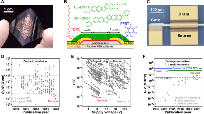
Fig. 1. Flexible organic transistors with small contact resistance and high-frequency performance.

(A) Photograph of organic TFTs and circuits fabricated at a maximum process temperature of 100°C on a flexible, transparent PEN substrate. (B) Schematic cross section of the TFTs and chemical structures of the organic materials used in their fabrication: n-tetradecylphosphonic acid (TDPA) used for the self-assembled monolayer (SAM) in the hybrid aluminum oxide/SAM gate dielectric, PFBT used to treat the gold source and drain contacts to reduce the contact resistance and the small-molecule organic semiconductors DPh-DNTT and C10-DNTT. (C) Photograph of a TFT having a channel length of 8 μm, a total gate-to-contact overlap of 4 μm, and a channel width of 200 μm. (D) Literature overview of the width-normalized contact resistance (RCW) in organic TFTs. The dotted lines at 102 and 105 Ω·cm indicate the typical range of contact resistances reported for organic TFTs. (E) Literature overview of the signal propagation delay per stage (τ) of organic TFT–based ring oscillators as a function of supply voltage. (F) Literature overview of the highest voltage-normalized transit frequencies (fT/V) of organic TFTs fabricated on rigid and flexible substrates. The solid horizontal lines indicate the voltage-normalized transit frequencies of LTPS TFTs used in smartphone displays and of state-of-the-art low-temperature–processed IGZO TFTs; the dashed line indicates approximately the minimum requirement for mobile displays (3 MHz V−1). For references, see table S1. (A and C) Photo credit: James W. Borchert, Max Planck Institute for Solid State Research.
