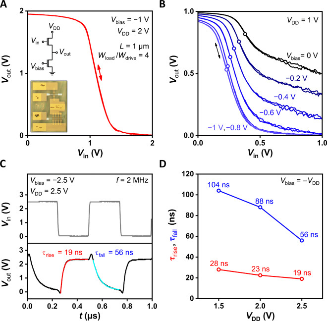
Fig. 3. Static and dynamic inverter characteristics.

(A) Static transfer characteristics of an inverter based on two DPh-DNTT TFTs in a biased-load circuit design fabricated on a flexible PEN substrate for a supply voltage (VDD) of 2 V and bias voltage (Vbias) of −1 V. The TFTs have a channel length (L) of 1 μm and a total gate-to-contact overlap of 4 μm. The insets show the circuit diagram and a photograph of the inverter. Photo credit: James W. Borchert, Max Planck Institute for Solid State Research. (B) Static transfer characteristics of the same inverter for bias voltages ranging from −1 to 0 V. The open circles indicate the trip voltage. (C) Dynamic characteristics of the inverter in response to a square-wave input signal with a frequency of 2 MHz, a duty cycle of 50%, and an amplitude of 2.5 V. Characteristic rise and fall time constants of the switching delays (τrise, τfall) were determined by fitting simple exponential functions to the measured output waveform. (D) Rise and fall time constants measured for supply voltages (VDD) of 1.5, 2.0, and 2.5 V. The amplitude of the square-wave input signal was identical to the supply voltage, and Vbias = −VDD for each measurement.
