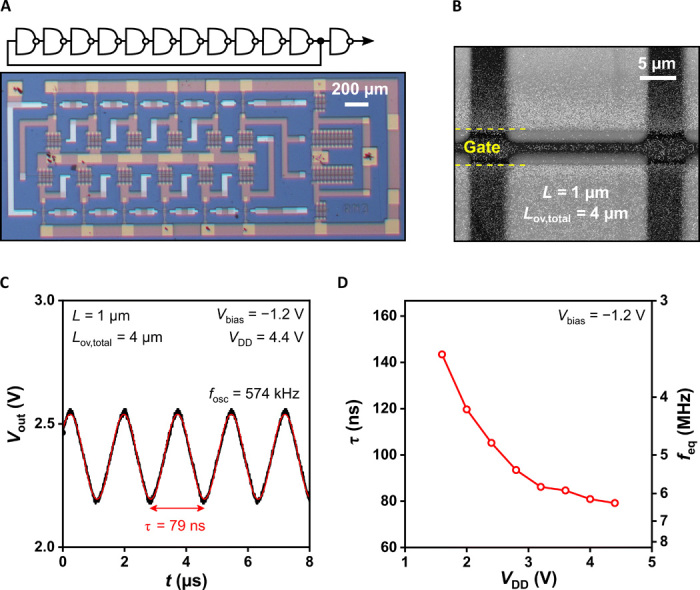
Fig. 4. Dynamic circuit characteristics.

(A) Circuit diagram and photograph of an 11-stage ring oscillator based on biased-load inverters fabricated on a PEN substrate. Photo credit: James W. Borchert, Max Planck Institute for Solid State Research. (B) SEM micrograph of the channel region of an individual C10-DNTT TFT in the ring oscillator. All TFTs in the circuit have a channel length (L) of 1 μm and a total gate-to-contact overlap (Lov,total) of 4 μm. (C) Measured output signal of the ring oscillator operated with a supply voltage (VDD) of 4.4 V. A signal-propagation delay per stage (τ) of 79 ns is determined by fitting a sine wave to the output signal. (D) Stage delay and equivalent frequency (feq = 1/2τ) plotted as a function of the supply voltage.
