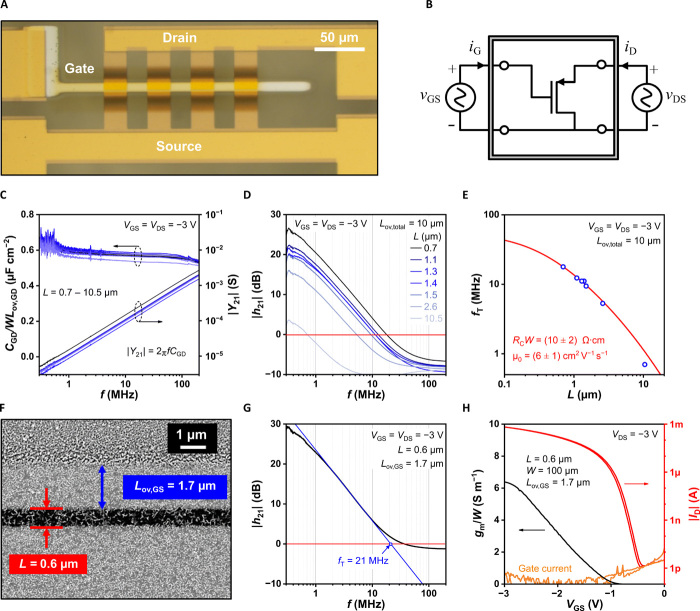
Fig. 5. Two-port network analysis of flexible organic transistors.
(A) Photograph of an organic TFT designed for two-port network analysis fabricated on a PEN substrate. All TFTs considered here have a total gate-to-contact overlap (Lov,total) of 10 μm and a channel width (W) of 100 μm. Photo credit: James W. Borchert, Max Planck Institute for Solid State Research. (B) Circuit diagram of a two-port network with a TFT as the device under test. (C) Drain component of the total gate capacitance (CGD) normalized by the gate-to-drain overlap area (WLov,GD) and plotted as a function of the measurement frequency (f) for all of the TFTs in the two-port network analysis. The gate-drain capacitance CGD was calculated from the measured admittance parameters (|Y21| = 2πfCGD). (D) Magnitude of the small-signal current gain (|h21|) of TFTs with channel lengths (L) ranging from 0.7 to 10.5 μm and with nominally identical gate-to-source and gate-to-drain overlaps (Lov,GS = Lov,GD) plotted as a function of the measurement frequency. The transit frequencies (fT) are determined as the frequency at which |h21| = 0 dB (red line). (E) Transit frequency (fT) plotted as a function of the channel length (L). The red line is a fit of Eq. 1 to the measurement data (blue circles), yielding a width-normalized contact resistance (RCW) of (10 ± 2) Ω·cm and an intrinsic channel mobility (μ0) of (6 ± 1) cm2 V−1 s−1. (F) SEM micrograph of the channel region of an asymmetric DPh-DNTT TFT with a channel length (L) of 0.6 μm, a gate-to-source overlap (Lov,GS) of 1.7 μm, and a gate-to-drain overlap (Lov,GD) of 8.3 μm. (G) Measured small-signal current gain (|h21|) of the same TFT plotted as a function of the measurement frequency, indicating a transit frequency (fT) of 21 MHz. (H) Measured transfer characteristics and transconductance (gm) plotted as a function of the gate-source voltage of the same TFT.

