Figure 1.
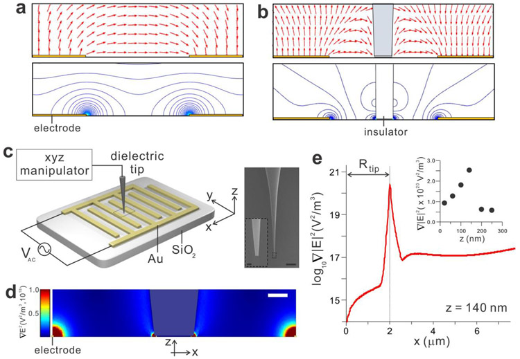
Insulator-based dielectrophoretic (iDEP) tweezers. (a) Electric field lines (red arrow) and contour plot of the field created by the metal electrodes. (b) Deformation of the field by the insulating obstacle in the center generates the additional iDEP trap. (c) Schematic diagram of the device and zoomed-in SEM images of the insulating tip controlled by the xyz manipulator. The scale bars are 500 μm and 2 μm (inset). (d) The distribution and the strength of the electric field gradient around the tip calculated by the finite element COMSOL simulation, predicting the strong field gradient at the electrode edges and the tip end. The scale bar is 5 μm. (e) The line profile of the electric field gradient along the x-axis at the tip height z of 140 nm, showing a very sharp peak of the field gradient at the rim of the tip. The inset presents the peak values of the field gradient’s strength as function of z.

