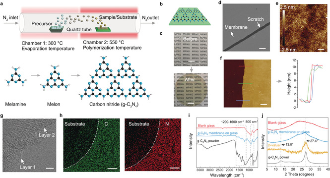
Figure 1.

a) Illustration showing the growth of ultrathin carbon nitride film by CVD onto surfaces. b) Idealized molecular structure of the g‐C3N4 film on a substrate. c) Quartz substrate before and after film polymerization. Scale bar: 1 cm. d) SEM images of a scratch in an otherwise continuous carbon nitride film on a silicon wafer substrate. Scale bar: 10 μm. e) Mean roughness of the film as determined by AFM is about 0.51 nm. Scale bar: 1 μm. f) Typical AFM height image of the film and the corresponding height profile over a scratch showing a thickness of about 10 nm. Scale bar: 1 μm. g) High‐resolution TEM of a free standing film indicating at least local crystallinity but full orientation with layers parallel to the surface. Scale bar: 10 nm. h) EDX analysis of carbon nitride film. Scale bar: 10 μm. i) FTIR of blank glass substrate, g‐C3N4 film on glass, and g‐C3N4 powder. j) XRD of blank glass substrate, g‐C3N4 film on glass, g‐C3N4 powder, and difference value (D‐value) between g‐C3N4 film on glass and blank glass substrate.
