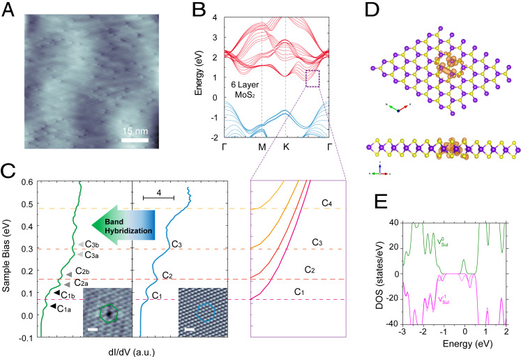
Fig. 1.
Electronic properties and band structure of six-layer MoS2 with sulfur vacancy. (A) Large-area STM image of the bare MoS2 on h-BN substrate (VS = 1.0 V, I = 0.7 nA). The dark topographic contrast, which shows the single sulfur vacancy features, can be found over the whole scanned area. (B) DFT calculation of six-layer MoS2. The zoomed-in image shows the conduction subbands (Cn) near the CBM at point of six-layer MoS2. (C) dI/dV spectrum (VS = −0.7 V, I = 1.3 nA) at the vicinity of a sulfur vacancy (Left side) (scale bar, 0.6 nm) and pristine region (Right) (scale bar, 0.8 nm) of MoS2 near CBM. Conduction subbands C1, C2, and C3 can be revealed from the resonance peaks in STS curve of pristine MoS2. However, each of those subbands split into two bands (Cna and Cnb) due to band hybridization in the vicinity of a sulfur vacancy. (D) Top and side views of spin density associated with single sulfur vacancy in monolayer MoS2. (Purple larger spheres represent molybdenum atoms, and smaller yellow spheres represent sulfur atoms.) The spin density associated with VSul−1, with a significant component localized at the three exposed Mo atoms. (E) Electronic DOS of the sulfur vacancy in neutral (VSul0) and −1 charged state (VSul−1) (for intuitive understanding, the VBMs for the two cases were aligned).The charging of the vacancy leads to the lifting of the degeneracy of defective level indicated by the splitting of curves of spin-up (dashed line) and spin-down (solid line) states for VSul−1.

