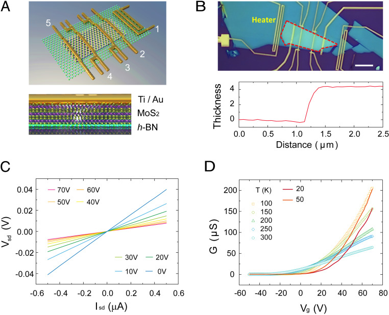
Fig. 2.
Structural and electronic properties of MoS2/h-BN heterostructure. (A) Schematic diagram of the device. Electrode 1 acts as an electrical heater. Electrodes 2 and 5 act as a current source for four-probe electrical measurements, while electrodes 3 and 4 act as thermometers. (Bottom) The section view of the heterostructure. (B) Optical image of a complete device. The dotted red dashed box outlines the MoS2 flake. (Scale bar, 10 μm.) (Bottom) AFM scan gives the thickness of MoS2 flakes as 4.2 ± 0.3 nm. (C) Four-probe Isd-Vsd curves at different Vg values at 300 K. (D) Four-probe FET characterization at different temperatures. Clear crossover can be found at for T > 100 K, which is defined as the MIT. For , MoS2 shows metallic behavior, and conductance decreases with increasing T. For , conductance increases with increasing T, which is a typical insulating behavior. When T < 100 K, the conductance (in the metallic region) drops anomalously as T decreases.

