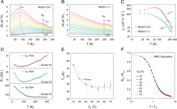
Fig. 3.
Carrier density and temperature-dependent properties of defective MoS2 on h-BN substrate. (A) Four-probe sheet conductivity of MoS2/h-BN devices as a function of T and Vg. MIT can be observed when σs ∼ e2/h. The anomalous peaks Tmax at low temperatures are marked out by the red dashed line. (B) Four-probe sheet conductivity of MoS2/SiO2 devices as a function of T and Vg. (C) Temperature-dependent field effect mobility. The solid line shows the phonon-limited power law . and for MOS2/SiO2 sample. For MoS2 on h-BN, and reaches . For T < 100 K, is observed for MoS2/h-BN sample indicating an anomalous scattering mechanism. (D) Temperature dependence of four-probe resistance at Vg = 70, 50, and 30 V for MoS2/h-BN device, with the resistance minima at 70, 89, and 135 K, respectively. (E) Gate tuning of the Kondo temperature Tk. (F) Normalized Kondo resistance versus normalized temperature for the data from Vg = 10 V to Vg = 70 V. The red dashed line describes the universal Kondo behavior from numerical renormalization group calculations (35).

