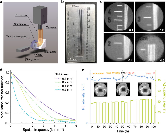
Fig. 3. X-ray imaging based on Cs2Ag0.6Na0.4In0.85Bi0.15Cl6 scintillator wafers with different thicknesses.
a Schematic of the X-ray imaging system. b Photograph of the standard X-ray test-pattern plate. c X-ray images of the test-pattern plate based on Cs2Ag0.6Na0.4In0.85Bi0.15Cl6 wafers with different thicknesses (dose rate: 189 μGyair s−1, voltage: 50 kV). d Corresponding MTF curves of Cs2Ag0.6Na0.4In0.85Bi0.15Cl6 wafers with different thicknesses. e Integrated RL intensity of Cs2Ag0.6Na0.4In0.85Bi0.15Cl6 under thermal treatment for 50 h at 85 °C followed by X-ray illumination for another 50 h (dose rate: 12 μGyair s−1, voltage: 50 kV). The moisture level was also recorded, and the RL was measured with an integrating sphere. The inset shows X-ray images of a circuit board acquired at three different stages (0 h, 50 h and 100 h) with a dose rate of 189 μGyair s−1 at a voltage of 50 kV

