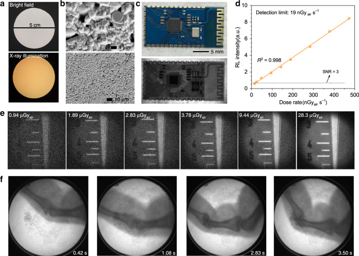
Fig. 4. Real-time and low-dose X-ray imaging with Cs2Ag0.6Na0.4In0.85Bi0.15Cl6 scintillator wafers.
a Photographs of a Cs2Ag0.6Na0.4In0.85Bi0.15Cl6 wafer under daylight and X-ray illumination (dose rate: 47.2 μGyair s−1, voltage: 50 kV). b SEM images of the wafer surface. c Photograph of a circuit board (top) and its X-ray image (below) (dose rate: 47.2 μGyair s−1, voltage: 50 kV). d RL intensity of Cs2Ag0.6Na0.4In0.85Bi0.15Cl6 measured at low-dose rates. The detection limit is derived from the fitting curve as the value when the SNR equals 3 (voltage: 50 kV). e X-ray images of the test-pattern plate acquired under different X-ray doses (voltage: 50 kV). f Real-time X-ray images of finger bending (dose rate: 47.2 μGyair s−1, voltage: 50 kV)

