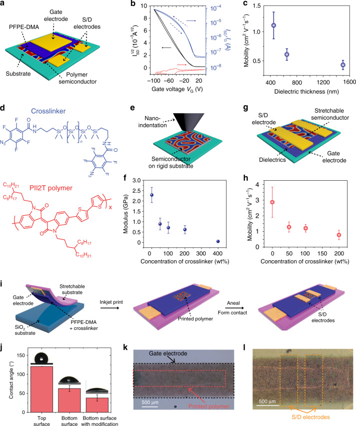
Fig. 2. Fully stretchable thin-film OTFTs.
a Schematic of the top-gate-bottom-contact (TGBC) structure of isoindigo-based PII2T polymer using the PFPE-DMA as the gate dielectric (thickness 500 nm to 1.5 µm and dielectric constant of ca. 2.2), Al/Au as gate electrode and Cr/Au as the source and drain (S/D) electrodes. W/L = 20, Vsd = 100. b Representative transfer characterization of the TGBC structure OTFTs. c The mobility value of OTFTs to the thickness of PFPE-DMA gate dielectrics. d Chemical structures of (PDMS)-azide crosslinker and PII2T semiconductor polymer as stretchable semiconductor ink for inkjet printing. The molecular weight of PDMS is 3100 g/mol. e Schematic of nanoindentation used for the Young’s modulus measurement. f Young’s modulus of the intrinsically stretchable semiconductor polymer to the concentration of the PDMS-azide crosslinker in PII2T polymer. g Schematic of the top-contact-bottom-gate (TCBG) device structure for measuring values of mobility. h The saturation mobility of OTFT as a function of the concentration of PDMS-azide crosslinker in PII2T polymer. The dielectric is octadecyltrichlorosilane (OTS) modified SiO2, the drain and source electrodes are thermally evaporated gold (40 nm) with W/L = 20. i Schematics of the stepwise process for the fabrication of a freestanding, fully stretchable OTFT array through inkjet printing. The gate electrode was prepared by spray using CNT/ Poly(3-hexylthiophene) (P3HT) with a thickness ~5 µm. The drain and source electrodes were prepared by spray coating using CNT/P3HT material with a thickness of ~10 µm. The W/L = 2. The PFPE dielectric layer thickness is 1.5 μm with a capacitance per area of 1.4 nF/cm2. j Statistical analysis of contact angle measurement for PFPE-DMA film with surface different modifications. Inset images show representative contact angle measurements for each condition. Top surface: top surface of PFPE-DMA film spin-coated on dextran/SiO2 substrate. Bottom surface: bottom surface of PFPE-DMA film spin-coated on dextran/SiO2 substrate. Bottom surface with modification: bottom surface of PFPE-DMA spin-coated on PDMS-azide/dextran/SiO2 substrate post-baked at 150 °C for 40. Values are mean ± S.D. k Optical bright-field (BF) image shows inkjet-printed semiconducting polymers on the PFPE-DMA gate dielectric layer with the bottom-gate electrode. l Optical BF image shows the thermal annealed semiconducting polymers patterned with top S/D CNT stretchable electrodes.

