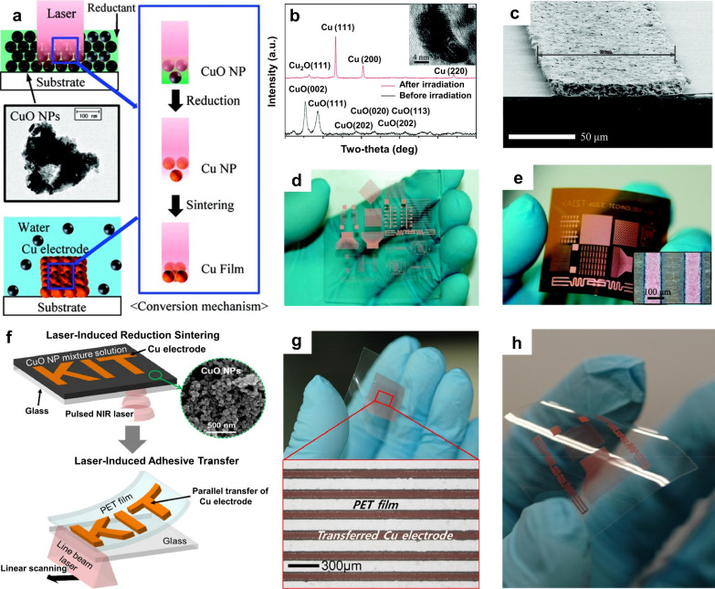
Fig. 5.
a Schematic of the proposed process for the conversion of CuO NPs into a Cu film via photochemical reduction and photothermal agglomeration. b XRD analysis results obtained before and after laser irradiation; (inset) TEM image of a Cu film processed using a pulsed laser. c Cross-sectional SEM image of the Cu electrode. d, e Photograph of Cu electrode patterns on a glass substrate and a PI substrate, respectively (a–e reproduced with permission from Ref. [77]. Copyright American Chemical Society 2011). f Schematic of the fabrication procedures for laser-induced reductive sintering and laser-induced adhesive transfer. g Photograph and microscope image of Cu NP electrodes transferred to a PET receiver film at a laser power of 2 W and a laser scanning speed of 2000 mm min−1. h Photograph of arbitrary Cu electrode patterns transferred to the PET film (f–h reproduced with permission from Ref. [81]. Copyright Elsevier, 2018)

