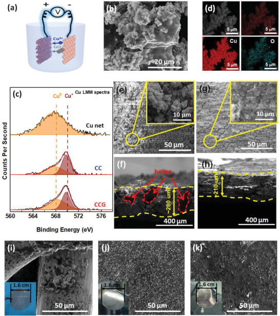
Figure 3.

a) Schematic representation of the set‐up for CCG/Cu synthesis. b) SEM image of the CCG composite. c) Auger Cu LMM spectra of Cu net, CC, and CCG. d) EDS mapping of the CC composite. e–h) Top and cross‐sectional SEM images of e,f) CC/Cu and g,h) CCG/Cu after 4 mAh cm−2 Li deposition. i–k) SEM images with corresponding digital photos of i) Cu net, j) CC/Cu, and k) CCG/Cu after immersion in molten Li.
