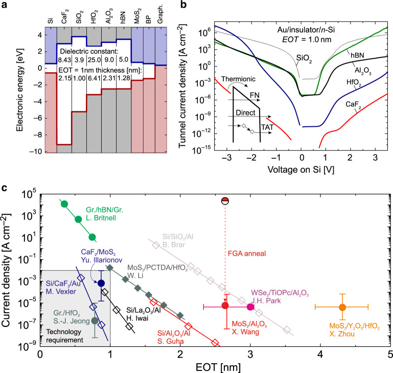
Fig. 3. Gate leakage currents through different insulators.
a Band diagram showing the alignment of the band gaps of some previously used insulators in 2D FETs relative to Si and typical 2D channel materials. b The leakage currents through the metal-insulator-semiconductor structures with these insulators for an EOT of 1 nm calculated using the WKB approach57 considering direct, FN tunneling and thermionic emission. The inset shows the important contributions to the tunneling current. For defective oxides, trap-assisted tunneling can lead to a significant contribution at low voltages, which is not accounted for in our best-case model. c Experimental gate leakage currents versus EOT measured at standard FET operating gate voltages 1–3 V. Literature data shown with open symbols for Si-based59–62 and filled symbols for 2D-based structures39,40,46,63–66.

