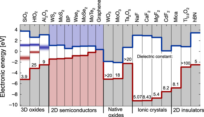
Fig. 6. Band diagram of different insulators matched with 2D semiconductors.

Left: energetic alignments of already known defect bands (gray areas) in several 3D oxides23,93,99,114 relative to the conduction and valence band edges of some frequently used 2D channel materials157 (center). Right: matching of potentially interesting native oxides, ionic crystals and 2D insulators with the same 2D channels. Note that HfO2 can be both a 3D oxide and the native oxide of HfS2 and HfSe2 and might have similar defect bands in both cases. The dielectric constants are given next to the valence band of the insulators while the numerical values are summarized in tabular form in Box 3. The zero energy would correspond with the Si midband.
