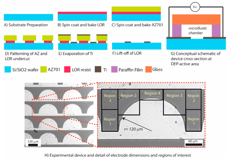
Figure 1.
Fabrication of Ti electrodes: (A) A six-inch silicon substrate was descummed with oxygen plasma treatment at 20 uTorr. (B) LOR resist was spin coated at 2000 rpm for 45 s on to the silicon substrate and a soft bake was performed at 150 °C for 150 s. (C) AZ701 resist was spin coated at 3000 rpm for 45 s on top of the LOR resist layer and a soft bake was performed at 110 °C for 75 s. (D) A Quintel Ultra i-line Series machine was used to pattern the resist layers using UV light with λ = 365 nm at an intensity of 6 mW/cm2 for 20 s. Pattern development was performed via immersion in a 2.3% tetramethylammonium hydroxide/97.7% water bath (E). The patterned silicon substrate was transferred to a CCS CA-40 E-beam Evaporator to deposit 350 nm of Ti. (F) Lastly, the wafer was immersed in NMP (1-methyl-2-pyrrolidone) to dissolve the AZ and LOR layers and effectively lift-off Ti from undesired regions of the substrate (Figure 1F). (G) Conceptual schematic of the cross section of an experimental device. (H) Experimental device and details of electrode dimensions and predefined regions of interest surrounding a single semicircular electrode.

