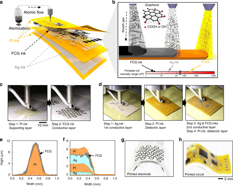
Fig. 1. Design, architecture, and nanomanufacturing of a p-NHE.
a, b Schematic illustrations of printing of aerosol nanoparticles from PI, Ag, and graphene inks to construct a multilayered structure. The atomized droplets in a N2 gas stream are directed to the print head to draw desired patterns on a substrate (a). The aerosol stream is controlled and delivered by a sheath gas to the substrate; three types of inks with different viscosity values are sequentially printed in this work (b). Small inset shows a chemical structure of graphene which is partially oxidized with carboxylic and hydroxyl groups. c Sequential photos of printing of PI and graphene ink to fabricate a stretchable nanomembrane electrode. In Step 1, PI ink is printed on a PMMA/glass substrate as a supporting layer. In Step 2, graphene ink is printed on top of the PI as a conductive layer for an electrode. d Still images showing a printing process of a multilayered biopotential recording circuit. In Step 1, Ag ink is deposited on a PI/PMMA/glass substrate as a circuit ground plane. In Step 2, PI ink is deposited as a dielectric layer except where the VIAs are located. In Step 3, Ag and FCG inks are printed as a metal interconnect layer that is connected to the ground plane. In Step 4, additional PI ink is printed to completely enclose the entire circuit except contact pads to integrate functional chip components. e, f Measured cross-sectional profiles of a printed stretchable electrode (e) and a printed multilayered circuit (f). g, h Close-up photos of the printed electrode (g) and circuit (h) on elastomeric membranes in e and f.

