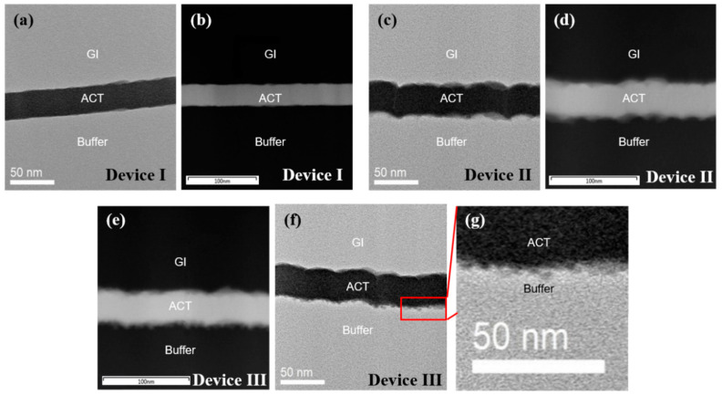
Figure 4.
High-resolution TEM (HR-TEM) images of the gate insulator (GI) (SiO2)/active (IGZO)/buffer (SiO2) interfaces for devices (a) I, (c) II and (f) III, respectively. Annular dark-field (ADF) images in a scanning TEM (STEM) for devices (b) I, (d) II and (e) III, respectively. (g) Enlarged interface of device III.

