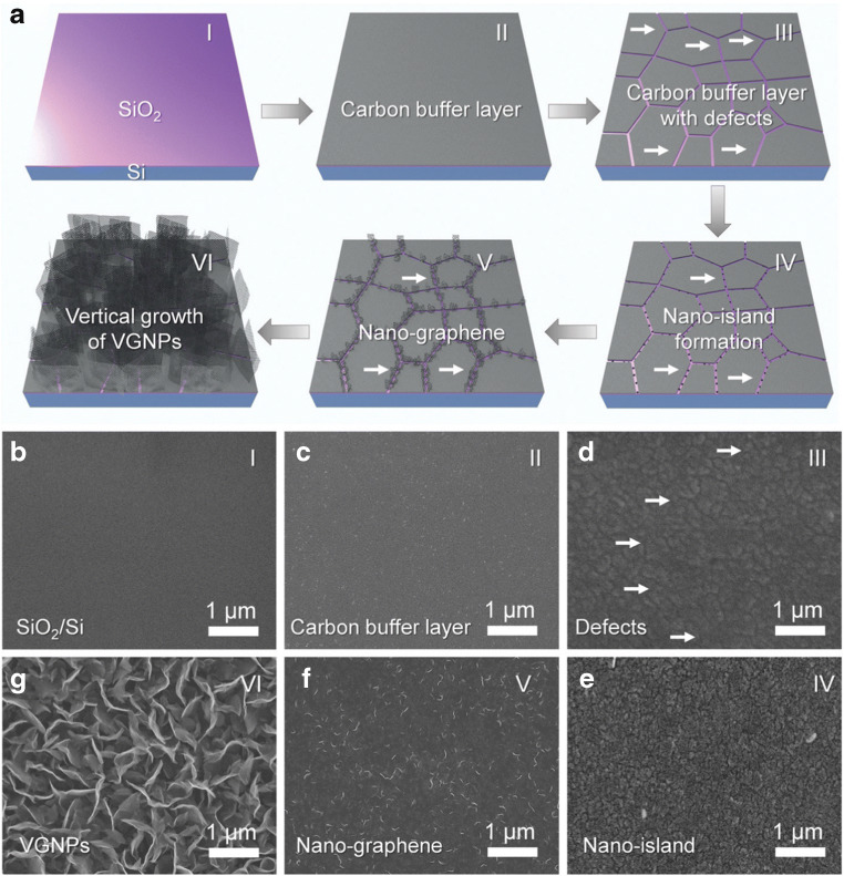
Fig. 4.
Illustration of the preparation process of graphene derived by plasma-assisted CVD growth (a). The numbers (I–IV) scheme the corresponding SEM images (b–g). The SiO2/Si support (I, b) was modified by depositing a carbon buffer layer (II, c), followed by the introduction of defects within the material (III, d) forming nanoislands (IV, e). At the edges of the nanoislands, the growth of graphene is initiated (V, f), resulting in the vertical growth of graphene flakes (VI, g). Reprinted from [58] with permission from The Royal Society of Chemistry

