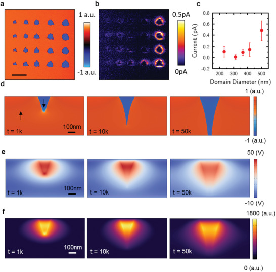
Figure 1.

a) Vertical piezoresponse force microscopy map of a 5 × 5 µm2 region of the 500 nm thick ion‐sliced lithium niobate single crystal, showing the combined vertical amplitude and phase response of the domain structure written using a stationary biased atomic force microscopy tip. b) Conductance map of the same region with −2.3 V DC bias applied to the bottom electrode. c) A plot of current against domain diameter, as measured at the top surface of the LiNbO3 thin film. Points represent mean currents obtained from the 100 datapoints at each domain size which showed the largest current values (error bars mark two standard deviations). d–f) Phase‐field simulation of d) domain evolution during tip‐induced switching in a 500 nm LiNbO3 film and corresponding e) electrostatic potential and f) electron density, estimated by using a degenerate electron gas approximation.
