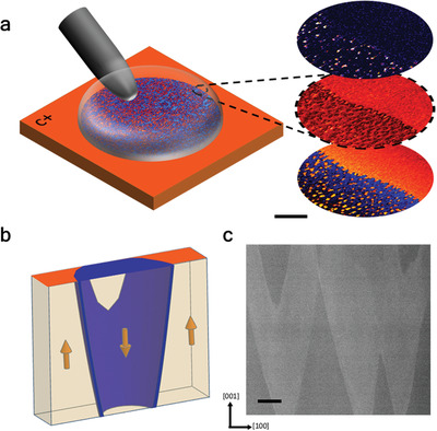
Figure 2.

a) Schematic showing a tungsten carbide needle electrically contacting microscopic Ga–In–Sn eutectic alloy electrodes to allow switching and conductance measurements at the mesoscale. The three images to the right are (top‐to‐bottom) typical current, piezo‐response amplitude and phase across the boundary between a partially switched and completely unswitched region. The fine‐scale microstructure and localized conducting domain walls are evident. The scale bar for the maps is 1 µm. b) 3D schematic showing typical domain structure in a lamella (arrows represent polarization directions) used for transmission electron microscopy investigations. c) Scanning transmission electron microscopy high angular annular dark field image (STEM‐HAADF) of a lamella cut from a partially switched region. The high density and angle of the domain walls can clearly be seen. The variations in contrast are associated with variations in the microstructure that occur through the thickness of the lamella: dark areas are associated with a uniform domain state (either “up” or “down”) throughout the entire lamellar thickness (cream regions in the schematic shown in (b), while lighter areas are associated with both “up” and “down” domains and the domain wall being sampled by the electron beam in the through‐thickness direction (in the schematic shown in b, these would be areas in which the blue domain wall is sampled in the through‐thickness direction). Scale bar 50 nm.
