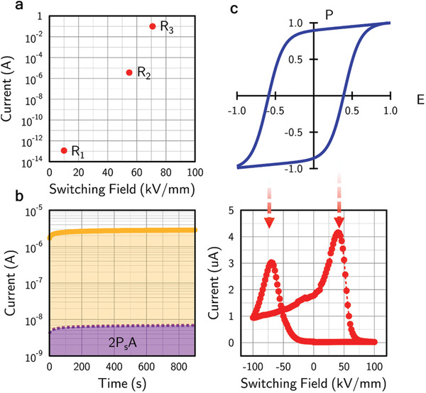
Figure 3.

a) Three different conduction states induced during initial switching studies, spanning twelve orders of magnitude in resistance. The current measured for the R3 state hit the compliance limit of the source‐measure unit, implying that even greater resistance changes during switching are likely to occur. b) Steady‐state current (measured at 10 kV mm−1) in a high conductance state (yellow/orange) compared with the equivalent switching current based on the maximum possible switching charge discharged over the 900 s measurement period (purple). Clearly, the dc currents observed cannot be accounted for by domain wall movement. c) A schematic hysteresis loop compared with the conductance measured as a function of switching field. Currents were measured at 5 V (equivalent field of 10 kV mm−1) applied for 1000 ms and the switching field was applied stroboscopically (in between each dc current measurement) in 10 ms pulses. Arrows indicate the relation between the current peaks (states of highest conductance) and the coercive field in the P–E loop. Note the slight imprint which causes off‐centring of the P–E response and an asymmetry in the switching fields needed to generate the most highly conducting states.
