
Figure 4.
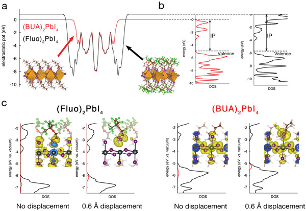
a) Electrostatic potential along the thickness of (BUA)2PbI4 and (Fluo)2PbI4 slabs; b) Partial density of electronic states (pDOS) for the two materials referred to the electrostatic potential in (a). The ionization potential (IP) is indicated. c) Total density of state (black curve) and density of state (red line) of one iodine which has been pulled out by 0.6 Å (vide infra) with respect to the central PbI4 plane. The spatial localization of the valence band edge orbital is reported in the inset.