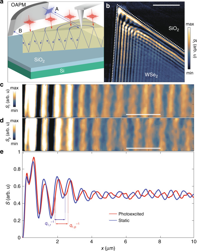
Fig. 1. Time resolved infrared nano-imaging experiments on WSe2.
a Nano-imaging experiments are performed in a tr-SNOM set-up by shining probe radiation (blue) onto the apex of the AFM tip. Radiation back scattered from the tip-apex (beam A) is collected by an off-axis parabolic mirror (OAPM) and sent to the detector. Simultaneously, a waveguide mode propagating through the crystal slab is launched. Upon reaching the sample edge waveguide modes are scattered to free space (beam B). A second pump channel (red) homogeneously perturbs the sample and alters the propagation of the waveguide modes. b Image of the near-field amplitude, Sr, at the WSe2/SiO2 interface. The edge of the WSe2 flake was determined from the topography and is indicated by the white dashed line. The scale bar is 5 μm in length. c Image of the near-field amplitude collected along the direction normal to an edge of WSe2 in the steady state. d Image of the near-field amplitude acquired with sample in its photoexcited state at the time delay of Δt = 1 ps. A pump with energy 1.58 eV and power 2.5 mW was applied to photo-excite the crystal. The scale bars in panels c and d are 2 μm in length and the images are co-located. e Averaging the 2D data of panels c and d yields line cuts of the scattering amplitude recorded under equilibrium (blue) and photoexcited (red) conditions, respectively. The experimental traces were vertically offset for clarity. The periodicity of the oscillations is characterized by wavevectors q1,r and q1,p under steady-state and photo-excited conditions respectively. Panels b-e were collected with the probe energy, E = 1.45 eV on WSe2 crystals with approximately 120 nm thickness.

