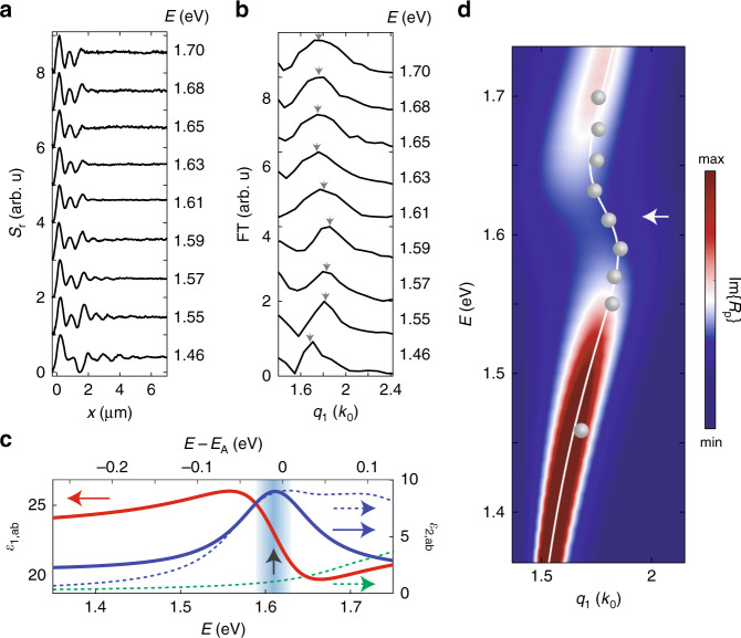
Fig. 2. Steady-state electrodynamics of the WSe2 crystal from spatio-temporal nano-imaging.
a Near-field scattering amplitude, Sr, at several probe energies (1.46–1.70 eV) plotted as a function of the real space coordinate relative to the edge of the 90 nm thick WSe2 crystal. b Fourier transforms of the data in panel a are shown in units of k0, the wavevector of light in free space, after angular correction (see Supplementary Note 2). The arrows indicate the real part of the dominant wavevector, q1,r (see Supplementary Notes 2–4). The data presented in panels a and b are offset for clarity. c The in-plane component of the dielectric function of bulk WSe2 (ε1,ab shown in red, ε2,ab shown in blue) obtained from a series of Lorentzian oscillators with parameters reported in Supplementary Table 1 (see Supplementary Note 8). The imaginary component of the dielectric function obtained from first principles calculations including excitonic effects (dashed blue curve) can be compared with the result obtained when excitonic effects are excluded (dashed green curve). The energy scale for the theoretical calculations is on the top, which was offset by the A-exciton energy (see Supplementary Note 8). The A-exciton energy, Ex, is indicated with a black arrow. d The energy versus momentum dispersion of the waveguide mode calculated with the in-plane component of the dielectric function represented by the Lorentz model (shown in panel c). The dispersion is represented with the imaginary component of the p-polarized reflection coefficient, Im{Rp} (false color map) along with the analytical solution (white line; Supplementary Notes 3, 4). The experimental results for q1,r vs. E extracted from the data of panels a and b are displayed with gray dots. The energy Ex is indicated with a white arrow.

