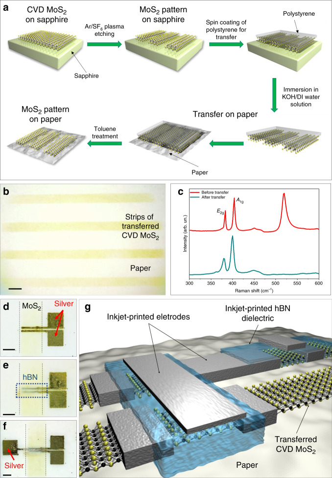
Fig. 1. Transferring scheme of MoS2 channel stripes and fabrication process of MoS2 FETs.
a Schematic representation of the patterning and transferring procedure employed to obtain MoS2 strips on paper. b Optical micrograph showing the transferred MoS2 strips on paper. The scale bar corresponds to 1 mm. c Raman spectra acquired on the as-grown MoS2 layer on rigid substrate (red line) and after MoS2 transfer to paper (cyan line). d–f Fabrication steps of the inkjet-printed transistors on paper: d Inkjet-printing of silver source and drain contacts. e Inkjet-printing of the hBN dielectric layer (defined by the blue-dotted frame). f Inkjet printing of silver top-gate contact. The scale bars in d–f correspond to 250 μm. g Sketch showing an inkjet-printed circuit on paper with CVD-grown MoS2 channel.

