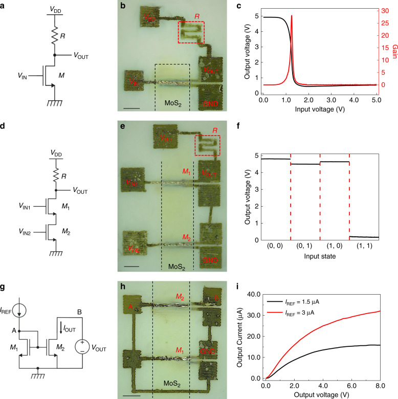
Fig. 4. Logic gates and current mirror based on inkjet-printed MoS2 FETs.
a Electrical schematic and b optical image of an inverter. c Output voltage (left axis) and voltage gain (right axis) of the inverter gate as a function of the input voltage. d Electrical schematic and e optical image of a NAND gate. f Output voltage of the NAND gate as a function of the input states (VIN1, VIN2). Voltage bias is 5 V for both the inverter and the NAND gate. g Electrical schematic and h optical image of a current mirror. i Output current of the current mirror as a function of the output voltage for two different values of the reference current. Legend: VDD, supply voltage; GDN, ground reference; VIN and VOUT, input and output voltage; M, inkjet-printed transistor. R, inkjet-printed graphene resistor. The scale bars in b, e, h correspond to 250 μm.

