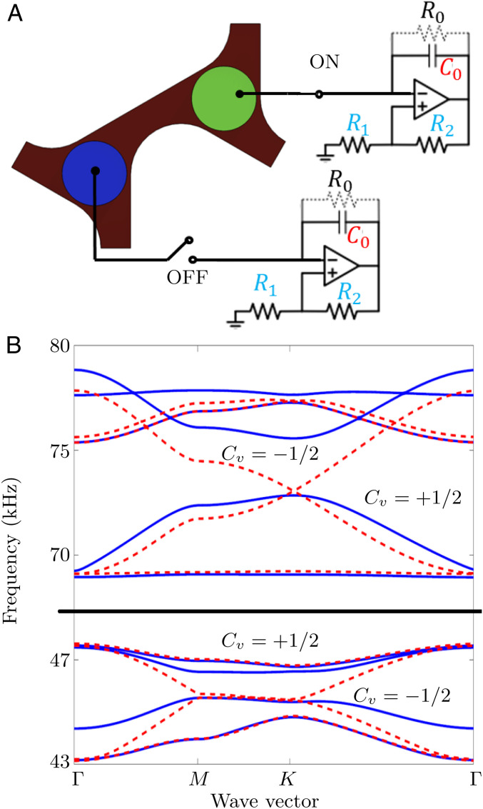
Fig. 1.
Phononic crystal band structure. (A) Schematic of the phononic crystal formed by hexagonal unit cells with PLA ( mm thick) as the host layer and attached circular PZT patches with thickness of mm ( mm in diameter) connected to external circuits. These circuits provide negative capacitance of . (B) Comparison between the band structures in the absence (red dashed curves with two Dirac points at 45 and 73 kHz) and in the presence (blue solid curves with optimal bandgap at nF) of completed external circuits attached to one PZT disk.

