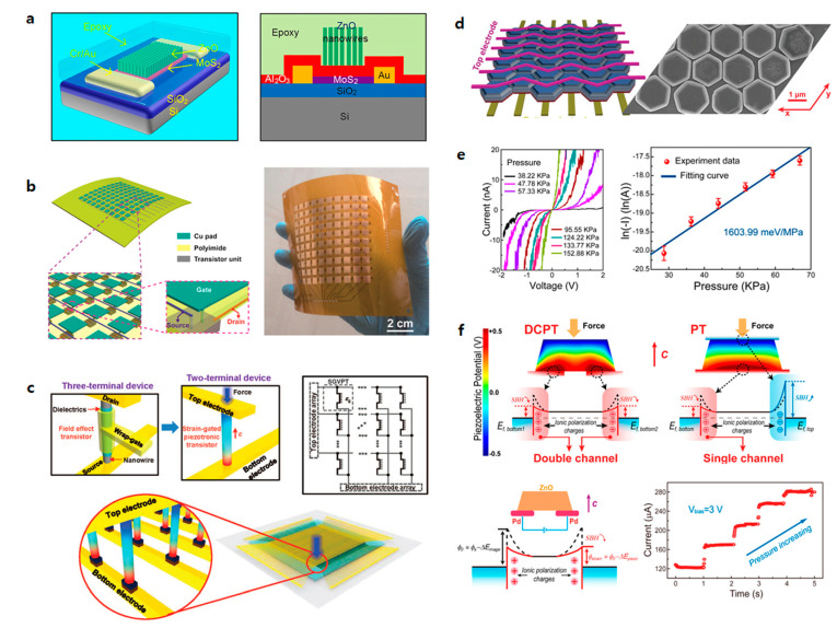
Figure 5.
Transistor array using pressure-sensitive channel materials. (a) Schematic illustration of a FET based on a MoS2 and ZnO heterostructure (left). Schematic cartoon graphs of the architecture of the device that uses the ZnO nanowire (NW) array and MoS2 flake, separated by a 20-nm atomic layer deposition (ALD)-deposited Al2O3 layer. (b) Schematic of a 10 × 10 tribotronic transistor array (TTA) (left). Partial enlarged tilted views of the TTA configuration and pixel structure, respectively (inset). Optical photograph of a fully integrated TTA with each sensing pixel of 5 × 5 mm (right). (c) Comparison between three-terminal voltage-gated NW FET and two-terminal strain-gated vertical piezotronic transistor (left). Color gradient in the strained strain-gated vertical piezotronic transistor (SGVPT) represents the strain-induced piezopotential field, in which red and blue indicate positive and negative piezopotential, respectively. ZnO NWs in SGVPT grow along the c axis (red arrow). Equivalent circuit diagram of the 3D SGVPT array (right). Equivalent circuit diagram of the 3D SGVPT array (bottom). The region highlighted by black dashed lines is the unit SGVPT device, in which εg represents the mechanical strain gate signal and the vertical dotted line between the two terminals of the SGVPT denotes the modulation effect of εg on the conducting characteristics of the device. (d) Schematic illustration of a 2D piezotronic transistor (2DPT) array using ZnO nanoplatelet (left). Scanning electron micrograph of 2DPT array with high spatial resolution (≈12,700 dpi) (right). (e) The modulation of carrier transport by pressure in a piezotronic transistor based on ZnO twin nanoplatelets, which shows the characteristic of piezotronic effect (left). ln(I)−P curve demonstrates a linear relationship between ln(I) and the applied pressure, showing the extreme sensitivity and indicating the modulation effect of applied pressure on conductance (right). (f) Piezopotential distributions and the corresponding energy-band diagrams of double-channel piezotronic transistor (DCPT) and conventional piezotronic transistor (PT) (top). Compared to one rise and another drop in conventional PT, both Schottky barriers in DCPT decrease with increasing pressure. Energy-band diagram of DCPT without (black dashed line) and with (red line) piezotronic effect, in which ΔEimage and ΔEpiezo represent mirror force and piezopotential-induced Schottky barrier height change, respectively (left). Current increased step-by-step with increasing pressure by a step of 63.5 kPa from 0.75 to 1.00 MPa at a fixed bias (right). (a) Reproduced with permission [86]. Copyright 2016, American Chemical Society (b) Reproduced with permission [89]. Copyright 2016, American Chemical Society. (c) Reproduced with permission [66]. Copyright 2013, American Association for the Advancement of Science. (d) Reproduced with permission [91]. Copyright 2017, American Chemical Society. (e) Reproduced with permission [88]. Copyright 2017, American Chemical Society. (f) Reproduced with permission [92]. Copyright 2018, American Chemical Society.

