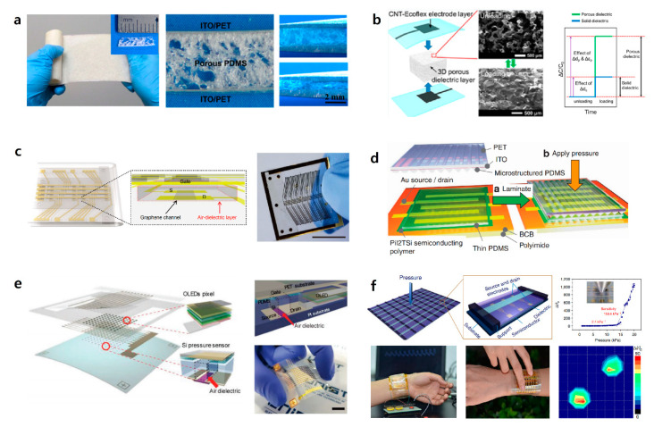
Figure 6.
Results of dielectric layer modification. (a) The photo image of the fabricated large area microstructured polydimethylsiloxane (PDMS) film (the inset shows the cross-sectional photo image of the microstructured PDMS film) (left); The cross-sectional photo images of the microstructured PDMS film clipped by a tweezer without pressure (upper) and with pressure (bottom) (right). (b) Relative changes in the capacitances of pressure sensors using solid and porous elastomeric dielectric layers induced by identical levels of external loading. The synergy of the larger deformation by the reduced stiffness and the increased effective dielectric constant by the closure of the air gap dramatically amplifies the capacitance change. (c) Schematic images of pressure-sensitive graphene FETs with air-dielectric layers after the folding. The air-dielectric layer is placed between the graphene channel and the gate electrode as illustrated in the schematic image (inset) (left); Photograph of the fabricated pressure-sensitive graphene FETs; scale bar, 1 cm (right). (d) Schematic of the final fabrication step of our pressure-sensitive transistor. (e) Schematic of active-matrix pressure-sensitive display, integrating the Si tactile pressure sensors and organic light-emitting diodes (OLEDs). (f) Suspended gate organic thin-film transistor pressure sensors. (a) Reproduced with permission [94]. (b) Reproduced with permission [95]. Copyright 2016, ACS Applied Materials & Interfaces. (c) Reproduced with permission [67]. Copyright 2017, Nature Communications. (d) Reproduced with permission [93]. Copyright 2013, Nature Communications. (e) Reproduced with permission [16]. Copyright 2019, Advanced Material Technologies. (f) Reproduced with permission [96]. Copyright 2015, Nature Communications.

