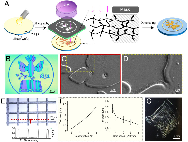
Fig. 2.
Microfabrication with PSF. (A) Fabrication scheme using PSF as a negative photoresist, whereby an arbitrary pattern (e.g., Tufts logo) may be achieved by selective cross-linking of the PSF by conventional lithography followed by a developing step to wash away the unreacted material. (B) Optical image of a PSF Tufts logo pattern and (C and D) SEM expansions of regions in dotted boxes. (E) Optical image of PSF cross-bar pattern on glass substrate. (Inset) The curve represents the height profile of structures shown in red dashed line. (F) PSF film thickness as a function of PSF photoresist solution concentration (n = 15) or spin speed during spin coating (n = 4). (G) Photo of a highly flexible, freestanding PSF construct achieved through etching underlying zinc relief layer.

